Marking of SMD components
Surface mount components are too small to bear standard markings on their housings. Therefore, there is a special system for designating such components: a code consisting of two or three characters is applied to the body of the device. The reference material provides information on more than 1500 codes.
Housing types and pinouts
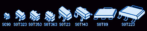
The most common miniature package for low-power diodes, diode assemblies and transistors is probably the three-terminal SOT23, made of plastic. For diodes, two-terminal packages SOD123, SOD323 and subminiature ceramic SOD110 are often used; Sometimes alphanumeric markings are not applied to them, then the type of device can be determined by the color of the strip at the cathode terminal. Transistors, diode and varicap assemblies are placed in three-lead packages SOT323, SOT346, SOT416, SOT490, subminiature SOT663, as well as in four-terminal packages SOT223, SOT143, SOT343 and SOT103. Five-pin packages are also used, for example, SOT551A and SOT680-1, in which the collector and/or emitter pins are duplicated for ease of wiring of printed circuit boards. Miniature six-pin packages, for example SOT26A, house transistor assemblies and diode matrices. Drawings of the most common SMD housings are shown in the figure.
Some devices have a variety with a reverse pinout and, accordingly, the letter “R” (Reveres) in the marking. Their conclusions correspond to the conclusions of a conventional device turned upside down, i.e. mirror image. Identification is usually done by code, but some manufacturers use the same code. In this case, you will need a strong magnifying glass. Typically, the terminals of housings (for example, such as SC 59, SC-70, SOT-323) come out closer to the front surface, and for inverted type devices, the terminals are located closer to the bottom side of the device housing. The exceptions are the SO-8, SOT-23, SOT-143 and SOT-223 cases, for them everything is the other way around.
How to use the information provided
To identify an SMD component, you need to determine the type of case and read the identification code printed on it. Next, you should find the designation in the alphabetical list of codes. Unfortunately, some codes are not unique. For example, a component labeled 1A could be either BC846A or FMMT3904. Even the same manufacturer may use the same codes to designate different components. In such cases, the housing type should be taken into account for more accurate identification.
Various encoding options
Many manufacturers use additional characters as their own identification code. For example, components from Philips usually (but unfortunately not always) have a lowercase "p" in addition to the code; components from Siemens usually have an additional lowercase
the letter "s". For example, if a component has code 1 Ap, you should look in the table for code 1 A. According to Table 1, there are four different options.
But since the component has the suffix “p”, it is manufactured by Philips, which means it is BC846A.
Many new Motorola components have a superscript after the code - small letters, for example SAC. These letters are just the month the device was manufactured. Many devices from Rohm Semiconductors starting with the letter G are equivalent to devices with markings equal to the rest of the code. For example, GD1 is the same as 01, that is, BCW31.
Some devices have a single colored letter (usually diodes in miniature packages). The color, if it has a meaning, is indicated in the table in brackets after the code or separately - instead of the code. It can be somewhat difficult to identify different types of housings for the same device. For example, 1K in a SOT23 package is BC848B (power 250 mW), and 1K in a SOT323 package is BC848BW (power 200 mW). In the tables presented, such devices are usually considered to be equivalent.
The suffix "L" usually indicates a low-profile case, such as the SOT323 or SC70, while the "W" indicates a smaller version of the case, such as the SOT343.
Analogue devices and additional information
Where possible, the listing indicates a type of conventional (non-SMD) device that has equivalent characteristics. If such a device is generally known, then no other information is given. For less common devices, additional information is provided. If a similar device does not exist, a brief description of the device is provided that may be helpful in selecting a replacement.
When describing the properties of a component, some parameters specific to a particular device are used. Thus, the voltage specified for a rectifying diode is most often the maximum peak reverse voltage of the diode, and for zener diodes the stabilization voltage is given. Usually, if voltages, currents or powers are indicated, these are limit values. For transistors, the area of application, operating range or cutoff frequency is indicated. For pulse diodes - switching time. For varicaps - the operating range and/or limits of capacitance change.
Some types of transistors (so-called “digital”) have built-in resistors. In this case, the “+” sign indicates a resistor connected in series with the base; without the “+” sign - a resistor that shunts the base-emitter junction. When two resistances are specified (separated by a slash), then the first of them is the resistance of the base resistor, the second is the resistance of the resistor between the base and emitter.
Table 1. Various encoding options
|
Description and/or analogue |
|||
|
p-MOS,20V,0.9A |
Codes SMD components starting with the number - 1
- Introduction
- SMD component housings
- Standard sizes of SMD components
- SMD resistors
- SMD capacitors
- SMD coils and chokes
- SMD transistors
- Marking of SMD components
- Soldering SMD components
Introduction
The modern radio amateur now has access to not only ordinary components with leads, but also such small, dark parts that you can’t understand what’s written on them. They are called "SMD". In Russian this means "surface mount components". Their main advantage is that they allow the industry to assemble boards using robots that quickly place SMD components in their places on the printed circuit boards, and then mass bake them to produce assembled printed circuit boards. The human share remains with those operations that the robot cannot perform. Not yet.
The use of chip components in amateur radio practice is also possible, even necessary, as it allows you to reduce the weight, size and cost of the finished product. Moreover, you practically won’t have to drill.
For those who first encountered SMD components, confusion is natural. How to understand their diversity: where is the resistor, and where is the capacitor or transistor, what sizes do they come in, what types of SMD parts are there? You will find answers to all these questions below. Read it, it will come in handy!
Chip component housings
Quite conventionally, all surface-mount components can be divided into groups according to the number of pins and housing size:
| pins/size | Very very small | Very small | Little ones | Average |
| 2 outputs | SOD962 (DSN0603-2) , WLCSP2*, SOD882 (DFN1106-2) , SOD882D (DFN1106D-2) , SOD523, SOD1608 (DFN1608D-2) | SOD323, SOD328 | SOD123F, SOD123W | SOD128 |
| 3 pins | SOT883B (DFN1006B-3) , SOT883, SOT663, SOT416 | SOT323, SOT1061 (DFN2020-3) | SOT23 | SOT89, DPAK (TO-252), D2PAK (TO-263), D3PAK (TO-268) |
| 4-5 pins | WLCSP4*, SOT1194, WLCSP5*, SOT665 | SOT353 | SOT143B, SOT753 | SOT223, POWER-SO8 |
| 6-8 pins | SOT1202, SOT891, SOT886, SOT666, WLCSP6* | SOT363, SOT1220 (DFN2020MD-6), SOT1118 (DFN2020-6) | SOT457, SOT505 | SOT873-1 (DFN3333-8), SOT96 |
| > 8 pins | WLCSP9*, SOT1157 (DFN17-12-8) , SOT983 (DFN1714U-8) | WLCSP16*, SOT1178 (DFN2110-9) , WLCSP24* | SOT1176 (DFN2510A-10) , SOT1158 (DFN2512-12) , SOT1156 (DFN2521-12) | SOT552, SOT617 (DFN5050-32), SOT510 |
Of course, not all packages are listed in the table, since the real industry produces components in new packages faster than the standardization bodies can keep up with them.
The housings of SMD components can be either with or without leads. If there are no leads, then there are contact pads or small balls of solder (BGA) on the case. Also, depending on the manufacturer, parts may differ in markings and dimensions. For example, capacitors may vary in height.

Most SMD component housings are designed for installation using special equipment that radio amateurs do not have and are unlikely to ever have. This is due to the technology of soldering such components. Of course, with a certain persistence and fanaticism, you can solder at home.
Types of SMD housings by name
| Name | Decoding | number of pins |
| SOT | small outline transistor | 3 |
| SOD | small outline diode | 2 |
| SOIC | small outline integrated circuit | >4, in two lines on the sides |
| TSOP | thin outline package (thin SOIC) | >4, in two lines on the sides |
| SSOP | seated SOIC | >4, in two lines on the sides |
| TSSOP | thin seated SOIC | >4, in two lines on the sides |
| QSOP | Quarter size SOIC | >4, in two lines on the sides |
| VSOP | Even smaller QSOPs | >4, in two lines on the sides |
| PLCC | IC in a plastic case with leads bent to form a letter-shaped case J | >4, in four lines on the sides |
| CLCC | IC in a ceramic package with leads bent to form a letter-shaped package J | >4, in four lines on the sides |
| QFP | square flat case | >4, in four lines on the sides |
| LQFP | low profile QFP | >4, in four lines on the sides |
| PQFP | plastic QFP | >4, in four lines on the sides |
| CQFP | ceramic QFP | >4, in four lines on the sides |
| TQFP | thinner than QFP | >4, in four lines on the sides |
| PQFN | power QFP without leads with a pad for a radiator | >4, in four lines on the sides |
| BGA | Ball grid array. Array of balls instead of pins | pin array |
| LFBGA | low profile FBGA | pin array |
| C.G.A. | housing with input and output terminals made of refractory solder | pin array |
| CCGA | CGA in ceramic case | pin array |
| μBGA | micro BGA | pin array |
| FCBGA | Flip-chip ball grid array. Man array of balls on a substrate to which a crystal with a heat sink is soldered | pin array |
| LLP | leadless housing |
From this whole zoo of chip components that can be used for amateur purposes: chip resistors, chip capacitors, chip inductors, chip diodes and transistors, LEDs, zener diodes, some microcircuits in SOIC packages. Capacitors usually look like simple parallelipipeds or small barrels. The barrels are electrolytic, and the parallelepipeds will most likely be tantalum or ceramic capacitors.

Standard sizes of SMD components
Chip components of the same denomination may have different dimensions. The dimensions of an SMD component are determined by its “standard size”. For example, chip resistors have standard sizes from “0201” to “2512”. These four digits encode the width and length of the chip resistor in inches. In the tables below you can see the standard sizes in millimeters.
smd resistors

| Rectangular chip resistors and ceramic capacitors | |||||
| Standard size | L, mm (inch) | W, mm (inch) | H, mm (inch) | A, mm | W |
| 0201 | 0.6 (0.02) | 0.3 (0.01) | 0.23 (0.01) | 0.13 | 1/20 |
| 0402 | 1.0 (0.04) | 0.5 (0.01) | 0.35 (0.014) | 0.25 | 1/16 |
| 0603 | 1.6 (0.06) | 0.8 (0.03) | 0.45 (0.018) | 0.3 | 1/10 |
| 0805 | 2.0 (0.08) | 1.2 (0.05) | 0.4 (0.018) | 0.4 | 1/8 |
| 1206 | 3.2 (0.12) | 1.6 (0.06) | 0.5 (0.022) | 0.5 | 1/4 |
| 1210 | 5.0 (0.12) | 2.5 (0.10) | 0.55 (0.022) | 0.5 | 1/2 |
| 1218 | 5.0 (0.12) | 2.5 (0.18) | 0.55 (0.022) | 0.5 | 1 |
| 2010 | 5.0 (0.20) | 2.5 (0.10) | 0.55 (0.024) | 0.5 | 3/4 |
| 2512 | 6.35 (0.25) | 3.2 (0.12) | 0.55 (0.024) | 0.5 | 1 |
| Cylindrical chip resistors and diodes | |||||
| Standard size | Ø, mm (inch) | L, mm (inch) | W | ||
| 0102 | 1.1 (0.01) | 2.2 (0.02) | 1/4 | ||
| 0204 | 1.4 (0.02) | 3.6 (0.04) | 1/2 | ||
| 0207 | 2.2 (0.02) | 5.8 (0.07) | 1 | ||
smd capacitors
Ceramic chip capacitors are the same size as chip resistors, but tantalum chip capacitors have their own size system:

| Tantalum capacitors | |||||
| Standard size | L, mm (inch) | W, mm (inch) | T, mm (inch) | B, mm | A, mm |
| A | 3.2 (0.126) | 1.6 (0.063) | 1.6 (0.063) | 1.2 | 0.8 |
| B | 3.5 (0.138) | 2.8 (0.110) | 1.9 (0.075) | 2.2 | 0.8 |
| C | 6.0 (0.236) | 3.2 (0.126) | 2.5 (0.098) | 2.2 | 1.3 |
| D | 7.3 (0.287) | 4.3 (0.170) | 2.8 (0.110) | 2.4 | 1.3 |
| E | 7.3 (0.287) | 4.3 (0.170) | 4.0 (0.158) | 2.4 | 1.2 |
smd inductors and chokes
Inductors are found in many types of housings, but the housings are subject to the same size law. This makes automatic installation easier. And it makes it easier for us, radio amateurs, to navigate.
All kinds of coils, chokes and transformers are called “winding products”. Usually we wind them ourselves, but sometimes you can buy ready-made products. Moreover, if SMD options are required, which come with many bonuses: magnetic shielding of the housing, compactness, closed or open housing, high quality factor, electromagnetic shielding, wide range of operating temperatures.

It is better to select the required coil according to catalogs and the required standard size. Standard sizes, as for chip resistors, are specified using a four-number code (0805). In this case, “08” indicates the length, and “05” the width in inches. The actual size of such an SMD component will be 0.08x0.05 inches.
smd diodes and zener diodes
Diodes can be either in cylindrical cases or in cases in the form of small parallelipipeds. Cylindrical diode packages are most often represented by MiniMELF (SOD80 / DO213AA / LL34) or MELF (DO213AB / LL41) packages. Their standard sizes are set in the same way as for coils, resistors, and capacitors.

| Diodes, Zener diodes, capacitors, resistors | |||||
| Type of shell | L* (mm) | D* (mm) | F* (mm) | S* (mm) | Note |
| DO-213AA (SOD80) | 3.5 | 1.65 | 048 | 0.03 | JEDEC |
| DO-213AB (MELF) | 5.0 | 2.52 | 0.48 | 0.03 | JEDEC |
| DO-213AC | 3.45 | 1.4 | 0.42 | - | JEDEC |
| ERD03LL | 1.6 | 1.0 | 0.2 | 0.05 | PANASONIC |
| ER021L | 2.0 | 1.25 | 0.3 | 0.07 | PANASONIC |
| ERSM | 5.9 | 2.2 | 0.6 | 0.15 | PANASONIC, GOST R1-11 |
| MELF | 5.0 | 2.5 | 0.5 | 0.1 | CENTS |
| SOD80 (miniMELF) | 3.5 | 1.6 | 0.3 | 0.075 | PHILIPS |
| SOD80C | 3.6 | 1.52 | 0.3 | 0.075 | PHILIPS |
| SOD87 | 3.5 | 2.05 | 0.3 | 0.075 | PHILIPS |
smd transistors
Surface mount transistors can also be of low, medium and high power. They also have matching housings. Transistor cases can be divided into two groups: SOT, DPAK.

I would like to draw your attention to the fact that such packages may also contain assemblies of several components, not just transistors. For example, diode assemblies.
Marking of SMD components
Sometimes it seems to me that the marking of modern electronic components has turned into a whole science, similar to history or archeology, since in order to figure out which component is installed on the board, sometimes you have to conduct a whole analysis of the elements surrounding it. In this regard, the Soviet output components, on which the denomination and model were written in text, were simply a dream for an amateur, since there was no need to rummage through piles of reference books to figure out what these parts were.
The reason lies in the automation of the assembly process. SMD components are installed by robots, in which special reels are installed (similar to the reels with magnetic tapes) in which chip components are located. The robot doesn’t care what’s in the bag or whether the parts are marked. Humans need labeling.
Soldering chip components
At home, chip components can only be soldered up to a certain size; size 0805 is considered more or less comfortable for manual installation. Smaller components are soldered using a stove. At the same time, for high-quality soldering at home, a whole range of measures should be observed.
There were circuits based on discrete electronic elements - resistors, transistors, capacitors, diodes, inductors, and they heated up during operation. And they still had to be cooled - a whole ventilation and cooling system was built. There were no air conditioners anywhere, people endured the heat, and all the machine rooms were ventilated and cooled centrally and continuously, day and night. And the energy consumption was megawatts. The computer's power supply occupied a separate cabinet. 380 volts, three phases, supply from below, from under the raised floor. Another cabinet was occupied by a processor. Another one is RAM on magnetic cores. And everything together occupied a hall of about 100 square meters. And the machine had RAM, scary to say, 512 KB.
And it was necessary to make computers more and more powerful.
Then they invented LSI - large integrated circuits. This is when the entire circuit is drawn in one solid form. A multilayer parallelepiped in which layers of microscopic thickness contain the same electronic elements drawn, sprayed or fused in a vacuum, only microscopic, and “crushed” into a plane. Usually the whole LSI is sealed in one housing, and then you are not afraid of anything - a piece of iron with a piece of iron, even hit with a hammer (just kidding).


Only LSI (or VLSI - very large integrated circuits) contain functional blocks or individual electronic devices - processors, registers, semiconductor memory units, controllers, operational amplifiers. And the task is to assemble them into a specific product: a mobile phone, a flash drive, a computer, a navigator, etc. But they are so small, these BIG integrated circuits, how to assemble them?
And then they came up with surface mounting technology.
Method for assembling complex electronic circuits SMT/TMP
Assembling microcircuits, LSIs, resistors, and capacitors on a board in the old fashioned way very soon became inconvenient and low-tech. And installation using traditional “end-to-end” technology became cumbersome and difficult to automate, and the results were not in accordance with the realities of the time. Miniature gadgets require miniature and, most importantly, easy-to-layout boards. Industry can already produce resistances, transistors, etc. that are very small and completely flat. All that was left to do was to make their contacts flat and pressed to the surface. And to develop technology for tracing and manufacturing boards as the basis for surface mounting, as well as methods for soldering elements to the surface. In addition to other advantages, they learned how to do soldering entirely - the entire board at once, which speeds up the work and ensures uniformity of its quality. This method is called " T technology m installation on P surface (TMP)", or surface mount technology (SMT). Since the mounted elements have become completely flat, in everyday life they are called “chips” or “chip components” (or also SMD - surface mounted device, for example, SMD resistors).
Steps for making a board using TMP
The production of a TMP board involves both the process of its design, manufacturing, selection of certain materials, and specific technical means for soldering chips onto the board.
- The design and manufacture of the board is the basis for installation. Instead of holes for through mounting, contact pads are made for soldering flat contacts of elements.
- Applying solder paste to pads. This can be done with a hand syringe or by screen printing for mass production.
- Precise placement of components onto the board over applied solder paste.
- Place the board with all components in the soldering oven. The paste melts and very compactly (thanks to additives that increase the surface tension of the solder) solders the contacts with the same quality over the entire surface of the board. However, the requirements for both operation time, temperature, and the accuracy of the chemical composition of materials are critical.
- Final processing: cooling, washing, applying a protective layer.


There are different technology options for serial and manual production. Mass production, subject to extensive automation and subsequent quality control, produces and guarantees high results.
However, SMT technology can also get along well with traditional mounting on a single board. In this case, manual SMT installation may be required.
SMD resistors
A resistor is the most common component in electronic circuits. There is even a specially designed circuitry that is built only from transistors and resistors (T-R logic). This means that it is possible to build a processor without the remaining elements, but without these two it is impossible. (Sorry, there is also TT logic, where there are generally only transistors, but some of them have to play the role of resistors). In the production of large integrated circuits they go to such extremes, but for surface mounting they still produce the entire set of necessary elements.

For such a compact assembly, they must have strictly defined dimensions. Each SMD device is a small parallelepiped with contacts protruding from it - legs, or plates, or metal tips on both sides. It is important that the contacts on the mounting side must lie strictly in a plane, and on this plane have the area necessary for soldering - also rectangular.

Resistor dimensions: l - length, w - width, h - height. The standard dimensions are taken to be the length and width that are important for installation.
They can be encoded in one of two systems: inch (JEDEC) or metric (mm). The conversion factor from one system to another is the length of an inch with mm = 2.54.
Standard sizes are encoded with a four-digit digital code, where the first two digits are the length, the second are the width of the device. Moreover, the dimensions are taken either in hundredths of an inch, or in tenths of a millimeter, depending on the standard.
And code 1608 in the metric system means 1.6 mm in length and 0.8 mm in width. By applying the conversion factor, it is easy to make sure that these are the same standard size. However, there are other dimensions that are determined by the size.

Chip resistor markings, ratings
Due to the small area of the device, special markings had to be invented to apply the usual value for resistors. There are two purely digital ones - three-digit and four-digit) and two alphanumeric (EIA-96), in which there are two numbers and a letter, and an encoding for resistance values less than 0, in which the letter R is used to indicate the position of the decimal point.
And there is one more special marking. A “resistor” without any resistance, that is, just a metal jumper, is marked 0, or 000.

Digital markings
Digital markings contain the exponent (N) of the multiplier (10 N) as the last digit, the remaining two or three are the mantissa of the resistance.
Resistor markings
Color coding of resistors
A simple calculator for calculating resistor values by color.
By clicking on the colors in the table, we color the resistor with stripes.
As a result, we get the value and tolerance of the resistor we need.
The first stripe from which the count is taken is usually wider or located closer to the resistor terminal.
Marking of SMD resistors
First of all, you should pay attention to the relatively new and not everyone is familiar with the EIA-96 marking standard, which consists of three characters - two numbers and a letter. The compactness of writing is compensated by the inconvenience of deciphering the code using a table.
Three-character marking EIA96
Coding of planar elements (SMD) in the standard EIA-96 provides for determining the value of three marking symbols for precision (high-precision) resistors with a tolerance of 1%.
The first two digits are the denomination code from 01
before 96
corresponds to the denomination number from 100
before 976
according to the table.
The third character is a letter - the multiplier code. Each of the letters X, Y, Z, A, B, C, D, E, F, H, R, S corresponds to the multiplier according to the table.
The resistor value is determined by the product of the number and the multiplier.
The principle of decoding SMD resistor standard codes E24 And E48 much simpler, does not require tables and is described separately below.
An online calculator for decoding resistors is offered EIA-96, E24, E48.
Three-character marking E24. Tolerance 5%
Three-digit marking. The first two digits are the denomination number.
The third digit is the decimal logarithm of the multiplier.
0=lg1, multiplier 1.
1=lg10, multiplier 10.
2=lg100, multiplier 100.
3=lg1000, multiplier 1000.
For this article, use the calculator window above as for EIA-96.
Four-character marking E48. Tolerance 2%
The marking consists of four numbers. The first three digits are the denomination number.
The fourth digit is the decimal logarithm of the multiplier.
0=lg1, multiplier 1.
1=lg10, multiplier 10.
2=lg100; Multiplier 100.
3=lg1000, multiplier 1000.
Etc., according to the number of zeros of the multiplier.
The product of the number and the multiplier will determine the resistor value.
You can use the input box below (only for E48), or enter 4 digits in the common top window.
Enter the SMD resistor code E48.
Enter the standard code EIA-96, or 3 digits E24, or 4 digits E48
Resistance:
Table EIA-96
|
Color coding of resistors, resistor calculator, SMD resistor calculator, resistor calculator by color stripes.
In amateur radio, not only ordinary radio components with leads, but also very small radio elements with incomprehensible inscriptions have received wide practical application. They are called "SMD", i.e. "surface mount radio parts". This reference material should help you understand the marking of SMD components.
All components of SMD installation can be divided into several groups according to the size of the case and the number of pins:
| pins/size | Very very small | Very small | Little ones | Average |
| 2 outputs | SOD962 (DSN0603-2) , WLCSP2*, SOD882 (DFN1106-2) , SOD882D (DFN1106D-2) , SOD523, SOD1608 (DFN1608D-2) | SOD323, SOD328 | SOD123F, SOD123W | SOD128 |
| 3 pins | SOT883B (DFN1006B-3) , SOT883, SOT663, SOT416 | SOT323, SOT1061 (DFN2020-3) | SOT23 | SOT89, DPAK (TO-252), D2PAK (TO-263), D3PAK (TO-268) |
| 4-5 pins | WLCSP4*, SOT1194, WLCSP5*, SOT665 | SOT353 | SOT143B, SOT753 | SOT223, POWER-SO8 |
| 6-8 pins | SOT1202, SOT891, SOT886, SOT666, WLCSP6* | SOT363, SOT1220 (DFN2020MD-6), SOT1118 (DFN2020-6) | SOT457, SOT505 | SOT873-1 (DFN3333-8), SOT96 |
| > 8 pins | WLCSP9*, SOT1157 (DFN17-12-8) , SOT983 (DFN1714U-8) | WLCSP16*, SOT1178 (DFN2110-9) , WLCSP24* | SOT1176 (DFN2510A-10) , SOT1158 (DFN2512-12) , SOT1156 (DFN2521-12) | SOT552, SOT617 (DFN5050-32), SOT510 |
Housings of SMD elements can be with or without leads. If there are no pins, then there are pads or very small balls of solder (BGA) on the package. In addition, all SMDs differ in dimensions and markings. For example, containers may have different heights.

Basically, the housings of SMD components are mounted using special equipment, which not every radio amateur has. But if you really want to, you can also solder BGA components into your home.
Surface Mount SMD Component Packages
Despite the huge number of standards regulating the requirements for chip packages, many manufacturers produce elements in packages that do not meet international standards. There are situations when a case with standard dimensions has a non-standard name.
Usually the name of the case consists of four numbers, which indicate its length and width. But some companies set these parameters in inches, while others set them in millimeters. For example, the name 0805 turns out like this: 0805 = length x width = (0.08 x 0.05) inches, and the case is 5845 (5.8 x 4.5) mm: Cases with the same name come in different heights (This is due to: for capacitors - the size of the capacitance and operating voltage, for resistors - power dissipation, etc.), different contact pads are made from various materials, but are designed for a standard installation location. The table below shows the dimensions in millimeters of the most popular types of housings.


Types of SMD enclosures by foreign names:

Of all this abundance of chip elements for a radio amateur, the following may be suitable: chip resistors, inductors, capacitors, diodes and transistors, LEDs, zener diodes, some microcircuits in SOIC design. The containers usually resemble simple parallelipipeds or small barrels. The barrels are electrolytic capacitors, and the parallelepipeds are tantalum or ceramic.

Marking of SMD components resistors |
All surface mount chip resistors are usually marked. Except for the resistances in the 0402nd case, since they are not marked due to their miniature size. Resistors of other sizes are marked using two main methods. If chip resistors have a resistance tolerance of 2%, 5% or 10%, then their marking consists of 3 digits: the first two indicate the mantissa, and the third is a power for the decimal base, i.e., the value of the resistor resistance in Ohms is obtained. For example, the resistance code is 106 - the first two digits 10 are the mantissa, 6 is the power, as a result we get 10x10 6, that is, 10 Mohm. Sometimes the Latin letter R is added to the digital marking - it is an additional multiplier and denotes a decimal point. SMD resistors of size 0805 and larger have an accuracy of 1% and are designated by a four-digit code: the first three are the mantissa, and the last is the power for the decimal base. The Latin symbol R can also be added to this marking. For example, the resistance code 3303 - 330 is the mantissa, 3 is the power, as a result we get 330x10 3, i.e. 33 kOhm. The code marking of SMD resistances with a tolerance of 1% and size 0603 is indicated by just two numbers and a letter using a table. The numbers indicate the code by which the mantissa value is selected from it, and the letter indicates the multiplier with a decimal base. For example, code 14R - the first two digits are 14 - this is the code. According to the table for code 14, the value of the mantissa is 137, R is a power equal to 10 -1, as a result we get 137x10 -1, that is, 13.7 Ohms. Resistors with zero resistance (jumpers) are simply marked with the number 0.
Each semiconductor device - SMD transistor - has its own unique designation or marking, by which it can be identified from a bunch of other CHIP components.
Marking of SMD diodes |


