From other circuits in one device is called galvanic isolation or isolation. With the help of such insulation, a signal or energy is transferred from one electrical circuit to another, without direct contact between the circuits.
Galvanic isolation makes it possible to ensure independence of the signal circuit, since an independent current circuit of the signal circuit is formed from other circuits, in feedback circuits and during measurements. For electromagnetic compatibility, galvanic isolation is the optimal solution, as the accuracy of measurements increases and the protection against interference increases.
Operating principle
To understand the principle of operation of galvanic isolation, let's consider how it is implemented in the design.
The primary winding is electrically isolated from the secondary winding. There is no contact between them, and no current arises, unless, of course, you count the emergency mode with an insulation breakdown or a turn short circuit. However, the potential difference in the coils can be significant.
Kinds
Such insulation of electrical circuits is ensured by various methods using all kinds of electronic elements and parts. For example, capacitors and optocouplers are capable of transmitting electrical signals without direct contact. Sections of the circuit interact through light flux, magnetic or electrostatic field. Let's consider the main types of galvanic insulation.
Inductive decoupling
To build a transformer (inductive) isolation, it is necessary to use a magnetic induction element called. It can be either with or without a core.
When decoupling the transformer type, transformers with a transformation ratio equal to unity are used. The primary coil of the transformer is connected to the signal source, the secondary coil is connected to the receiver. To decouple circuits using this scheme, magnetic modulation devices based on transformers can be used.
In this case, the output voltage, which is available on the secondary winding of the transformer, will directly depend on the voltage at the input of the device. There are a number of serious disadvantages with this inductive decoupling method:
- Significant overall dimensions that do not allow the manufacture of a compact device.
- Frequency modulation of galvanic isolation limits the transmission frequency.
- The quality of the output signal is affected by interference in the input carrier signal.
- The operation of transformer isolation is possible only with alternating voltage.
Optoelectronic isolation
The development of electronic and information technologies currently increases the possibility of designing an interchange using optoelectronic nodes. The basis of such decoupling units are optocouplers (optocouplers), which are made on the basis of, and other light-sensitive components.

In the optical part of the circuit, which connects the receiver and the data source, photons act as signal carriers. The neutrality of photons makes it possible to perform electrical decoupling of the output and input circuits, as well as to match circuits with different resistances at the output and input.
In optoelectronic isolation, the receiver does not influence the signal source, so it is possible to modulate signals over a wide frequency range. An important advantage of optical pairs is their compactness, which allows their use in microelectronics.
An optical pair consists of a light emitter, a medium that conducts the light flux, and a light receiver that converts it into an electric current signal. The output and input resistance of the optocoupler is very high, and can reach several million Ohms.
The principle of operation of the optocoupler is quite simple. A light flux comes out from and is directed to, which perceives it and carries out further work in accordance with this light signal.
In more detail, the operation of the optocoupler is as follows. The input signal is sent to an LED, which emits light through a light guide. Next, the light flux is perceived by a phototransistor, at the output of which a drop or pulse of electric current is created. As a result, galvanic isolation of circuits is performed, which are connected on one side to the LED, and on the other to the phototransistor.
Diode optocoupler
In this pair, the light source is an LED. Such a pair can be used instead of a key and work with signals with a frequency of several tens of MHz.
When it is necessary to transmit a signal, the source supplies power to the LED, resulting in the emission of light that hits the . When exposed to light, the photodiode opens and allows current to pass through it.

The receiver perceives the appearance of current as an operating signal. The disadvantage of diode optocouplers is the inability to control high currents without auxiliary elements. Another disadvantage is their low efficiency.
Transistor optocoupler
Such optical pairs have increased sensitivity, unlike diode ones, and therefore are more economical. But their reaction speed and highest connection frequency are lower. Transistor optical pairs have low resistance when open and high resistance when closed.

The control currents for the transistor pair are higher than the output current of the diode pair. Transistor optocouplers can be used in different ways:
- No base output.
- With base output.
Without a base lead, the collector current will be directly related to the LED current, but the transistor will have a long response time since the base circuit is always open.
In the case of a base output, it is possible to increase the reaction speed by connecting an auxiliary resistance between the emitter and the base of the transistor. An effect then occurs in which the transistor does not go into conduction until the diode current reaches the value required to drop the voltage across the resistor.
This galvanic isolation has several advantages:
- Wide range of decoupling voltages (up to 0.5 kV). This plays a big role in the design of information input systems.
- Galvanic isolation can operate at high frequencies, reaching several tens of MHz.
- The components of such an interchange circuit have small overall dimensions.
In the absence of galvanic insulation, the maximum current that passes between the circuits can be limited only by small electrical resistances. As a result, this leads to the emergence of equalizing currents that cause harm to the elements of the electrical circuit and to the worker who accidentally touches unprotected electrical equipment.
The series of articles consists of three parts:
Interference in circuits.
During normal operation of an electronic device, interference may occur in the circuit.
Interference can not only interfere with the normal operation of the device, but also lead to its complete failure.
Rice. 1. Interference in the useful signal.
You can see the interference on the oscilloscope screen by including it in the part of the circuit under study (Fig. 1). The duration of interference can be either very short (a few nanoseconds, so-called “needles”) or very long (several seconds). The shape and polarity of the interference also varies.
The propagation (passage) of interference occurs not only along the wire connections of the circuit, but sometimes even between parts of the circuit that are not connected by wires. In addition, interference can overlap and add up to each other. Thus, a single weak interference may not cause a malfunction in the device circuit, but the simultaneous accumulation of several weak random interferences leads to incorrect operation of the device. This fact makes the search and elimination of interference many times more difficult, since it takes on an even more random nature.
Sources of interference can be roughly divided:
- External source of interference. A strong electromagnetic or electrostatic field source near the device may cause the electronic device to malfunction. For example, a lightning discharge, relay switching of high currents or electric welding.
- Internal source of interference. For example, when you turn on/off a reactive load (an electric motor or an electromagnet) in a device, the rest of the circuit may malfunction. An incorrect program algorithm can also be a source of internal interference.
To protect against external interference, the structure or its individual parts are placed in a metal or electromagnetic shield, and circuit solutions with less sensitivity to external interference are also used. The use of filters, optimization of the operating algorithm, changes in the construction of the entire circuit and the location of its parts relative to each other help against internal interference.
What is considered very elegant is not the indiscriminate suppression of all interference, but the deliberate direction of them to those places in the circuit where they will fade out without causing harm. In some cases, this path is much simpler, more compact and cheaper.
Assessing the probability of interference in circuits and ways to prevent them is not a simple task, requiring theoretical knowledge and practical experience. But nevertheless, we can firmly say that the probability of interference increases:
- with an increase in switched current or voltage in the circuit,
- with increasing sensitivity of parts of the circuit,
- with an increase in the performance of the used parts.
In order not to redo the finished design due to frequent failures, it is better to become familiar with the possible sources and paths of interference at the circuit design stage. Since about half of all manifestations of interference are associated with “bad” power supply, it is best to start designing a device by choosing a method for powering its parts.
Interference in power supply circuits.
Figure 2 shows a typical block diagram of an electronic device, which consists of a power source, control circuit, driver and actuator.
Most of the simplest robots from the series on this site are built according to this scheme.

Rice. 2. Joint power supply of the control and power parts.
In such circuits we can conditionally distinguish two parts: control and power. The control part consumes relatively little current and contains any control or computing circuits. The power section consumes significantly more current and includes an amplifier and termination load.
Let's look at each part of the circuit in more detail.
Rice. 2 a.
Power supply(Fig. 2 a.) can be “batteries” or a mains transformer power supply. The power supply may also include a voltage stabilizer and a small filter.
Rice. 2 b.
Control circuit- this is part of the circuit (Fig. 2 b.), where any information is processed in accordance with the operation of the algorithm. Signals from external sources, for example, from some sensors, can also come here. The control circuit itself can be assembled using microcontrollers or other microcircuits, or using discrete elements.
Communication lines they simply connect the control circuit to the driver-executive device, that is, these are just wiring or tracks on a printed circuit board.
Rice. 2nd century
Actuator(Fig. 2 c.) is often a mechanism that converts an electrical signal into mechanical work, such as an electric motor or electromagnet. That is, the actuator converts electrical current into another form of energy and usually consumes a relatively large current.
Rice. 2 years
Since the signal from the control circuit is very weak, so driver or amplifier(Fig. 2 d) is an integral part of many schemes. The driver can be made, for example, using only a transistor or a special chip, depending on the type of actuator.
As a rule, the main source of strong interference is the actuator. The interference that appears here, having passed through the driver, spreads further along the power bus (The interference in Fig. 2 is shown schematically by an orange arrow). And since the control circuit is powered from the same power source, there is a high probability that this interference will affect it as well. That is, for example, an interference that appears in the motor will pass through the driver and can lead to a failure in the control circuit.
In simple circuits, it is enough to place a large capacitor of about 1000 μF and a ceramic 0.1 μF capacitor in parallel with the power source. They will act as a simple filter. In circuits with consumption currents of about 1 ampere or more, to protect against strong interference of complex shapes, you will have to install a bulky, complex filter, but this does not always help.
In many circuits, the easiest way to get rid of the effects of interference is to use separate power supplies for the control and power parts of the circuit, that is, the use of the so-called separate power supply.
Although separate power supply is used not only to combat interference.
Separate meals.
In Fig. Figure 3 shows a block diagram of a certain device. This circuit uses two power supplies. The power part of the circuit is powered from power supply 1, and the control circuit is from power supply 2. Both power sources are connected by one of the poles; this wire is common to the entire circuit and signals are transmitted relative to it along the communication line.

Rice. 3. Separate power supply for the control and power parts.
At first glance, such a circuit with two power supplies looks cumbersome and complex. In fact, such separate power supply circuits are used, for example, in 95% of all household equipment. Separate power supplies there are just different windings of transformers with different voltages and currents. This is another advantage of separate power supply circuits: several units with different supply voltages can be used in one device. For example, use 5 volts for the controller, and 10-15 volts for the motor.
If you look closely at the diagram in Fig. 3, it can be seen that interference from the power part does not have the opportunity to get into the control part via the power line. Consequently, the need to suppress or filter it completely disappears.

Rice. 4. Separate power supply with stabilizer.
In mobile structures, for example, mobile robots, due to their size, it is not always convenient to use two battery packs. Therefore, separate power supply can be built using one battery pack. The control circuit will be powered from the main power source through a stabilizer with a low-power filter, Fig. 4. In this circuit, you need to take into account the voltage drop across the stabilizer of the selected type. Typically a battery pack with a higher voltage than the voltage required for the control circuit is used. In this case, the functionality of the circuit is maintained even when the batteries are partially discharged.

Rice. 5. L293 with separate power supply.
Many driver chips are specifically designed for use in circuits with separate power supply. For example, the well-known L293 driver chip ( Rice. 5) has a conclusion Vss- for powering the control circuit (Logic Supply Voltage) and output Vs- to power the final stages of the power driver (Supply Voltage or Output Supply Voltage).
In all robot designs with a microcontroller or a logic chip from the series, L293 can be switched on with a separate power supply circuit. In this case, the power supply voltage (voltage for the motors) can be in the range from 4.5 to 36 volts, and the voltage on Vss can be supplied the same as to power the microcontroller or logic chip (usually 5 volts).
If the power supply to the control part (microcontroller or logic chip) occurs through a stabilizer, and the power supply to the power part is taken directly from the battery pack, then this can significantly save energy losses. Since the stabilizer will only power the control circuit, and not the entire structure. This - Another advantage of separate power supply: energy saving.
If you look again at the diagram in Figure 3, you will notice that in addition to the common wire (GND), the power section is also connected to the control circuit by communication lines. In some cases, these wires can also carry interference from the power part into the control circuit. In addition, these communication lines are often highly susceptible to electromagnetic influences (“noise”). You can get rid of these harmful phenomena once and for all by using the so-called galvanic isolation.
Although galvanic isolation is also used not only to combat interference.
Galvanic isolation.
At first glance, this definition may seem incredible!
How can a signal be transmitted without electrical contact?
In fact, there are even two ways that allow this.
Rice. 6.
Optical signal transmission method based on the phenomenon of photosensitivity of semiconductors. For this, a pair of an LED and a photosensitive device (phototransistor, photodiode) is used, Fig. 6.

Rice. 7.
The LED-photodetector pair is located in isolation in one housing opposite each other. This is what this detail is called. optocoupler(foreign name optocopler), Fig. 7.
If current is passed through the optocoupler LED, the resistance of the built-in photodetector will change. This is how contactless signal transmission occurs, since the LED is completely isolated from the photodetector.
Each signal transmission line requires a separate optocoupler. The frequency of the optically transmitted signal can range from zero to several tens to hundreds of kilohertz.
Rice. 8.
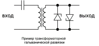
Inductive signal transmission method is based on the phenomenon of electromagnetic induction in a transformer. When the current changes in one of the windings of the transformer, the current in its other winding changes. Thus, the signal is transmitted from the first winding to the second (Fig. 8). This connection between the windings is also called transformer, and a transformer for galvanic isolation is sometimes called isolation transformer.
![]()
Rice. 9.
Structurally, transformers are usually made on a ring ferrite core, and the windings contain several tens of turns of wire (Fig. 9). Despite the apparent complexity of such a transformer, you can make it yourself in a few minutes. Ready-made small-sized transformers for galvanic isolation are also sold.
Each signal transmission line requires a separate such transformer. The frequency of the transmitted signal can range from several tens of hertz to hundreds of thousands of megahertz.
Depending on the type of signal being transmitted and the circuit requirements, you can choose either transformer or optical galvanic isolation. In circuits with galvanic isolation, special converters are often installed on both sides to coordinate (connect, interface) with the rest of the circuit.
Let us now consider the block diagram using galvanic isolation between the control and power parts in Figure 10.

Rice. 10. Separate power supply and galvanic isolation of the communication channel.
From this diagram it can be seen that any interference from the power part has no way of penetrating into the control part, since there is no electrical contact between the parts of the circuit.
The absence of electrical contact between parts of the circuit in the case of galvanic isolation allows you to safely control actuators with high voltage power. For example, a control panel powered by a few volts can be galvanically isolated from a phase network voltage of several hundred volts, which increases safety for operating personnel. This is an important advantage of galvanic isolation circuits.
Control circuits with galvanic isolation can almost always be found in critical devices, as well as in pulsed power supplies. Especially where there is even the slightest chance of interference. But even in amateur devices, galvanic isolation is used. Since a slight complication of the circuit by galvanic isolation brings complete confidence in the uninterrupted operation of the device.
Galvanic isolation or galvanic isolation is the general principle of electrical (galvanic) isolation of the electrical circuit in question in relation to other electrical circuits. Thanks to galvanic isolation, it is possible to transfer energy or a signal from one electrical circuit to another electrical circuit without direct electrical contact between them.
Galvanic isolation makes it possible to ensure, in particular, the independence of the signal circuit, since an independent current circuit of the signal circuit is formed relative to the current circuits of other circuits, for example, the power circuit, during measurements and in feedback circuits. This solution is useful for ensuring electromagnetic compatibility: noise immunity and measurement accuracy are increased. Galvanic isolation of the input and output of devices often improves their compatibility with other devices in harsh electromagnetic environments.
Of course, galvanic isolation also ensures safety when people work with electrical equipment. This is one measure, and the isolation of a particular circuit must always be considered in conjunction with other electrical safety measures, such as protective earthing and voltage and current limiting circuits.
To ensure galvanic isolation, various technical solutions can be used:
inductive (transformer) galvanic isolation, which is used in and for isolating digital circuits;
optical isolation by means of an optocoupler (optocoupler) or optorelay, the use of which is typical for many modern switching power supplies;
capacitive galvanic isolation, when the signal is supplied through a capacitor of a very small capacitance;
electromechanical isolation by means of, for example, .

Currently, two options for galvanic isolation in circuits are very widespread: transformer and optoelectronic.

The construction of transformer-type galvanic isolation involves the use of a magnetic induction element (transformer) with or without a core, the output voltage removed from the secondary winding of which is proportional to the input voltage of the device. However, when implementing this method, it is important to take into account the following disadvantages:
the output signal may be affected by interference generated by the carrier signal;
frequency modulation of the decoupler limits the transmission frequency;
large dimensions.

The development of semiconductor device technology in recent years has expanded the possibilities for constructing optoelectronic decoupling units based on optocouplers.
The principle of operation of the optocoupler is simple: the LED emits light, which is perceived by the phototransistor. This is how galvanic isolation of circuits is carried out, one of which is connected to the LED, and the other to the phototransistor.
This solution has a number of advantages: a wide range of decoupling voltages, up to 500 volts, which is important for building data input systems, the ability to operate decouplers with signals with frequencies up to tens of megahertz, and small dimensions of components.
If galvanic isolation is not used, the maximum current flow between circuits is limited only by relatively small electrical resistances, which can result in the flow of equalizing currents that can cause harm to both circuit components and people touching unprotected equipment. An isolation device specifically limits the transfer of energy from one circuit to another.
To switch loads in AC circuits, circuits using powerful field-effect transistors have recently begun to be increasingly used. This class of devices is represented by two groups. The first group includes bipolar transistors with an insulated gate - IGBT. The Western abbreviation is IGBT.
The second, most numerous, includes traditional field-effect (channel) transistors. This group also includes KP707 transistors (see Table 1), on which the load switch for a 220-volt network is assembled.
Primary AC power is a very dangerous thing in all respects. Therefore, there are many circuit solutions that avoid managing network loads directly. Previously, isolation transformers were used for these purposes; now they have been replaced by a variety of optocouplers.
Transistor switch with optical isolation
The scheme, which has already become standard, is shown in Figure 1. 
This circuit allows for galvanic isolation of the control circuits and the circuit of the primary 220 volt network. A TLP521 optocoupler is used as a decoupling element. You can use other imported or domestic transistor optocouplers. The scheme is simple and works as follows. When the voltage at the input terminals is zero, the optocoupler LED does not light up, the optocoupler transistor is closed and does not bypass the gate of the powerful switching transistors. Thus, at their gates there is an opening voltage equal to the stabilization voltage of the zener diode VD1. In this case, the transistors are open and operate in turn, depending on the polarity of the voltage at a given time. Suppose there is a plus at the output pin of circuit 4, and a minus at terminal 3. Then the load current will flow from terminal 3 to terminal 5, through the load to terminal 6, then through the internal protective diode of transistor VT2, through the open transistor VT1 to terminal 4. When the polarity of the supply voltage changes, the load current will flow through the diode of transistor VT1 and the open transistor VT2. Circuit elements R3, R3, C1 and VD1 are nothing more than a transformerless power supply. The value of resistor R1 corresponds to the input voltage of five volts and can be changed if necessary.
The entire circuit is made in the form of a functionally complete block. The circuit elements are mounted on a small U-shaped printed circuit board, shown in Figure 2. 
The board itself is attached with one screw to an aluminum plate with dimensions of 56x43x6 mm, which is the primary heat sink. Powerful transistors VT1 and VT2 are also attached to it through heat-conducting paste and mica insulating spacers using screws with bushings. The corner holes are aligned both in the board and in the plate and serve, if necessary, for attaching the unit to another more powerful heat sink.
Introduction
Galvanic isolation (isolation), commonly referred to simply as decoupling, is a method by which individual parts of an electrical system can be at different ground potentials. The two most common reasons for creating decoupling are for safety from faults in industrial-grade products, and where wired communication is required between devices, each of which has its own power supply.
Power decoupling methods
Transformers
The most common form of decoupling is the use of a transformer. When designing a power stabilization circuit where decoupling is required, the isolating part of the design is associated with the need to increase/decrease the voltage level and is not considered as a separate part of the system. In the event that it is necessary to isolate the entire electrical system (for example, many automotive test equipment requires power supplies to be isolated from the AC mains), a 1:1 transformer can be installed in series with the system to provide the necessary isolation.
Figure 1 - Assortment of SMD transformers
Capacitors
A less common method of creating decoupling is to use capacitors in series. Because of the ability for AC signals to flow through capacitors, this method can be an effective way to isolate parts of an electrical system from the AC mains. This method is less reliable than the transformer method because if a fault occurs, the transformer breaks the circuit and shorts the capacitor. One of the purposes of creating galvanic isolation from the AC mains is to ensure that in the event of a fault, the user is safe from a functioning unlimited current source.
Figure 2 - Example of using capacitors to create decoupling
Signal Isolation Methods
Opto-isolators
When a signal is required to pass between two parts of a circuit at different ground potentials, a popular solution is an opto-isolator (optocoupler). The opto-isolator is a phototransistor that opens (“turns on”) when the internal LED is energized. The light emitted by the internal LED is the signal path and thus the isolation between ground potentials is not broken.
Figure 3 - Diagram of a typical opto-isolatorHall Sensor
Another method of transmitting information between electrical systems with separate ground potentials is the use of a sensor based on the Hall effect. The Hall sensor detects induction non-invasively and does not require direct contact with the signal of interest and does not violate the insulating barrier. The most common use of passing inductive information through circuits at different ground potentials is in current sensors.
Figure 4 - Current sensor used to measure current through a conductor
Conclusion
Galvanic isolation (isolation) is the separation of electrical systems/subsystems that may not carry direct current and may have different ground potentials. Isolation can be divided into main categories: power and signal. There are several ways to achieve decoupling, and depending on the project requirements, some methods may be preferable to others.
Case Study
 Figure 5 - PoE (Power over Ethernet) project diagram based on the TPS23753PW controller
 In the diagram above, several transformers and an opto-isolator are used to create a switching power supply, which is used in Ethernet PD (Powered Device) devices. Connector J2 has internal magnets that isolate the entire system from the PoE source. T1 and U2 isolate the power supply (to the left of the red line) from the regulated 3.3V output (to the right of the red line).


